
As the semiconductor industry advances to 3nm, 2nm, and beyond, the demand for ultra-high-purity, high-performance materials that can withstand extreme manufacturing conditions has never been greater. Silicon Carbide (SiC) ceramics have become irreplaceable core components in wafer fabrication, offering unmatched high-temperature resistance, thermal shock stability, chemical inertness, and dimensional precision that traditional materials (alumina, quartz, metals) cannot match.This comprehensive product listing details our full line of SiC core components for semiconductor manufacturing, including lithography chucks, fixtures/trays, and cantilevers for diffusion furnaces. Each product is engineered to meet the strictest requirements of advanced semiconductor processes, ensuring wafer yield, production efficiency, and long-term equipment reliability.

Our SiC lithography chucks (also known as vacuum chucks or electrostatic chucks) are precision-engineered components custom-built for extreme-precision lithography machines. Designed to hold semiconductor wafers during the lithography process, these chucks deliver nanometer-level flatness and ultra-high cleanliness, enabling high-precision wafer adsorption and transport that is critical to maintaining chip fabrication accuracy.
Parameter
| Specification | |
Material | High-purity Recrystallized SiC (RSiC) / Reaction-Bonded SiC (SiSiC) |
Purity | ≥99.9% (ultra-low metal impurities <1ppm, compliant with SEMI standards) |
Flatness | ≤0.5μm per 300mm wafer, nanometer-level surface precision |
Surface Roughness | Ra ≤0.05μm (ultra-smooth, damage-free finish) |
Temperature Resistance | Continuous use up to 1600°C (RSiC) / 1350°C (SiSiC) |
Thermal Conductivity | ~150-200 W/m·K (excellent heat dissipation) |
Porosity | RSiC: 15-25% (optimized for vacuum adsorption); SiSiC: <0.5% (fully dense) |
Wafer Compatibility | 8-inch (200mm), 12-inch (300mm), and custom sizes |
Customization | Full customization of groove design, vacuum hole layout, and mounting interface |
Nanometer-Level Precision: Ultra-high flatness and surface finish eliminate wafer warpage and positioning errors, ensuring critical dimension (CD) accuracy in advanced lithography processes (EUV, DUV).
Ultra-High Cleanliness: Manufactured in a Class 100 cleanroom with strict impurity control, eliminating metal ion contamination that could damage sensitive semiconductor wafers.
Superior Vacuum Adsorption: Optimized porous structure for RSiC chucks delivers uniform, stable vacuum adsorption across the entire wafer surface, preventing slippage during high-speed scanning.
Extreme Thermal Stability: Low thermal expansion coefficient (4.0-4.5×10⁻⁶/K) matches silicon wafers, minimizing thermal stress and maintaining positioning accuracy during temperature fluctuations.
Long Service Life: 3-5 times longer service life than traditional ceramic or metal chucks, reducing equipment maintenance costs and production downtime.
Chemical Inertness: Resistant to all lithography process chemicals, photoresists, and cleaning agents, with no reaction or outgassing that could contaminate wafers.
EUV/DUV lithography machines for advanced logic and memory chip manufacturing
Wafer inspection and metrology equipment
High-precision wafer bonding and packaging processes
8-inch and 12-inch semiconductor wafer production lines
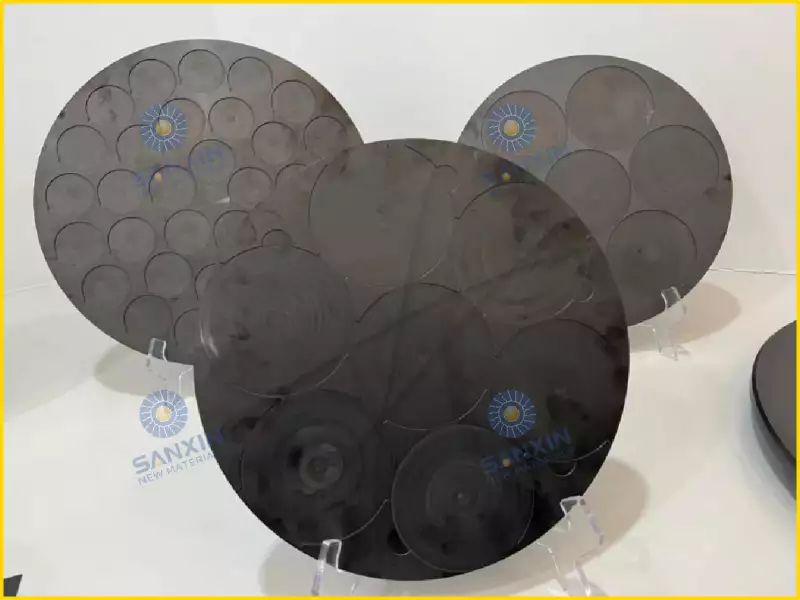
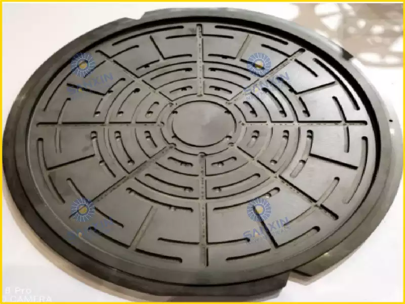
SiC fixtures and trays are high-performance process components designed for semiconductor etching, deposition, annealing, and diffusion processes. Manufactured from high-density reaction-bonded SiC (SiSiC) or recrystallized SiC (RSiC), these fixtures provide a contamination-free, high-temperature-resistant platform for wafer processing, ensuring consistent process results and wafer safety.
Parameter
| Specification | |
Material | High-density Reaction-Bonded SiC (SiSiC) / High-purity Recrystallized SiC (RSiC) |
Purity | 92-95% SiC (SiSiC) / ≥99.9% (RSiC), ultra-low metal impurities |
Temperature Resistance | Continuous use up to 1350°C (SiSiC) / 1600°C (RSiC) |
Hardness (Mohs) | 9.2 (second only to diamond, exceptional wear resistance) |
Flexural Strength | 300-400 MPa (SiSiC) / 100-200 MPa (RSiC) |
Plasma Etch Resistance | Ultra-high resistance to fluorine-based and chlorine-based plasmas |
Open Porosity | <0.5% (SiSiC, fully dense) / 15-25% (RSiC) |
Wafer Capacity | Customizable for 1-50+ wafers, compatible with 8-inch and 12-inch wafers |
Customization | Full customization of shape, slot design, and wafer holding structure |
Exceptional Plasma Resistance: Dense SiSiC structure delivers outstanding resistance to plasma etching, minimizing particle generation and component erosion in harsh plasma environments.
Zero Metal Contamination: Chemically inert to all process gases and chemicals, eliminating metal ion contamination of wafers, a critical requirement for advanced chip manufacturing.
Uniform Heat Distribution: High thermal conductivity ensures consistent temperature distribution across the tray, eliminating local overheating and ensuring uniform wafer processing.
High Load-Bearing Capacity: High mechanical strength supports heavy wafer loads in vertical and horizontal furnace systems, with no deformation during long-term high-temperature operation.
Thermal Shock Stability: Withstands rapid heating/cooling cycles (≥50°C/min) without cracking, ideal for annealing and rapid thermal processing (RTP) applications.
Long Service Life: 3-5 times longer service life than traditional quartz or alumina trays, reducing replacement costs and production downtime.
Semiconductor wafer etching (dry etching, plasma etching)
Chemical Vapor Deposition (CVD) and Physical Vapor Deposition (PVD) processes
High-temperature annealing and diffusion furnaces
Wafer cleaning and surface treatment processes
Advanced packaging (3D IC, Fan-Out) thermal processing
SiC cantilevers are precision load-bearing and conveying components specifically designed for semiconductor wafer diffusion furnaces, oxidation furnaces, and annealing furnaces. These cantilevers ensure stable, uniform wafer transport in high-temperature processes, directly improving wafer yield and production consistency.
Parameter
| Specification | |
Material | High-purity Recrystallized SiC (RSiC) / Reaction-Bonded SiC (SiSiC) |
Purity | ≥99.9% (RSiC, <1ppm metal impurities) / 90-95% SiC (SiSiC) |
Temperature Resistance | RSiC: Continuous use up to 1600°C; SiSiC: Continuous use up to 1350°C |
Thermal Shock Resistance | No cracking under rapid temperature change (≥50°C/min) |
Flexural Strength | RSiC: 100-200 MPa; SiSiC: 250-500 MPa |
Dimensional Tolerance | ±0.05mm (length), ±0.02mm (flatness) |
Surface Roughness | Ra ≤0.4μm (polished finish) |
Customization | Length (500mm-2000mm), cross-section, slot design fully customizable |
Ultra-High Purity: RSiC cantilevers feature ≥99.9% purity with ultra-low metal impurity content, eliminating contamination risks for sensitive semiconductor wafers in high-temperature diffusion processes.
Extreme High-Temperature Stability: Maintains structural integrity and dimensional accuracy without warpage or deformation during long-term furnace operation at 1300-1600°C.
Superior Thermal Shock Resistance: Optimized porous structure of RSiC absorbs thermal stress during rapid heating/cooling cycles, preventing cracking and extending service life to 3-5 years (3x longer than quartz cantilevers).
Precision Machining: Each cantilever is precision-ground and polished to ensure a smooth, burr-free surface, eliminating wafer scratching and breakage during transport.
Chemical Inertness: Resistant to all process gases (oxygen, nitrogen, hydrogen, dopant gases) and corrosive media, with no reaction or ion precipitation that could contaminate wafers.
Automation Compatibility: Dimensional precision and lightweight design ensure compatibility with automated wafer handling systems, supporting high-volume production.
Semiconductor wafer diffusion furnaces (phosphorus/boron diffusion for PN junction formation)
Oxidation and annealing furnaces for wafer thermal processing
Automated wafer handling systems in 8-inch and 12-inch wafer production lines
Advanced packaging and testing processes for high-performance chips
All our SiC core components share the following industry-leading advantages, making them the optimal choice for advanced semiconductor manufacturing:
Manufactured from high-purity SiC raw materials with strict impurity control, ensuring no metal ion contamination of sensitive semiconductor wafers.
Compliant with SEMI standards for semiconductor manufacturing materials, meeting the requirements of 3nm and below advanced process nodes.
Produced in Class 100 cleanrooms to eliminate particle contamination during manufacturing.
RSiC components withstand continuous operation up to 1600°C, SiSiC up to 1350°C, far exceeding the performance of traditional materials.
Low thermal expansion coefficient (4.0-4.5×10⁻⁶/K), matching the thermal properties of silicon wafers to minimize thermal stress and wafer warpage.
Superior thermal shock resistance, withstanding frequent thermal cycles without cracking or deformation.
High hardness (Mohs 9.2) and wear resistance ensure long-term dimensional accuracy and minimal wear, even in high-load, high-frequency production environments.
Service life of 3-5 years, 3-5 times longer than traditional alumina, quartz, and metal components, reducing total cost of ownership (TCO).
High mechanical strength for load-bearing components (fixtures, trays, cantilevers), supporting heavy wafer loads without deformation.
Inert to all semiconductor process gases, acids, alkalis, plasmas, and corrosive media, with no chemical reaction or impurity release.
Ideal for harsh process environments, including diffusion, etching, deposition, and cleaning processes.
No outgassing at high temperatures, ensuring process purity and wafer safety.
All components are fully customizable in size, shape, material, and surface finish to match specific equipment models, wafer sizes (8-inch, 12-inch), and process requirements.
Compatible with all major semiconductor equipment brands and automated production lines.
Custom design support for specialized processes (EUV lithography, high-temperature diffusion, plasma etching).
Material
Recrystallized SiC (RSiC) | Reaction-Bonded SiC (SiSiC) | |
Key Properties | High purity, high temperature resistance, thermal shock stability | High strength, low porosity, wear resistance, plasma resistance |
Max Operating Temperature | 1600°C | 1350°C |
Purity | ≥99.9% (ultra-high purity) | 90-95% SiC (with free silicon) |
Porosity | 15-25% (controlled open porosity) | <0.5% (fully dense) |
Flexural Strength | 100-200 MPa | 250-500 MPa |
Ideal Applications | Lithography chucks, diffusion furnace cantilevers, wafer carriers (direct wafer contact, high-temperature processes) | Fixtures, trays, furnace liners, structural components (load-bearing, plasma processes, non-direct wafer contact) |
All our SiC components are manufactured under strict ISO 9001 quality management systems, with full traceability from raw material to finished product. We provide comprehensive quality testing, including:
Purity analysis (ICP-MS) for ultra-low metal impurities
Dimensional inspection, flatness, and surface roughness testing
High-temperature performance and thermal shock testing
Vacuum leak testing for chucks and adsorption components
Plasma etch resistance testing for fixtures and trays
Compliance with SEMI international standards for semiconductor materials
Silicon Carbide (SiC) ceramics are the foundational materials enabling the next generation of semiconductor manufacturing. From precision lithography chucks that ensure nanometer-level accuracy, to high-strength fixtures and trays for harsh plasma processes, to reliable cantilevers for high-temperature diffusion furnaces, our SiC components deliver unmatched performance, purity, and reliability.These components directly drive improvements in wafer yield, production efficiency, and chip performance, making them essential for advanced semiconductor fabs worldwide. Whether you require custom SiC lithography chucks for EUV machines, high-performance SiC fixtures for etching processes, or reliable cantilevers for diffusion furnaces, we provide tailored solutions to meet your specific manufacturing requirements.
A: RSiC is optimized for ultra-high purity and high-temperature resistance (up to 1600°C), ideal for components in direct contact with wafers (lithography chucks, cantilevers). SiSiC offers higher mechanical strength, density, and plasma resistance, perfect for load-bearing structural components (fixtures, trays) at moderate temperatures (up to 1350°C).
A: SiC’s high purity eliminates contamination, while its thermal stability and low thermal expansion reduce wafer warpage and breakage. The uniform heat distribution and precision design ensure consistent process results, directly improving wafer yield by 1-3% in high-volume production.
A: Under normal operating conditions, SiC components have a service life of 3-5 years, 3-5 times longer than traditional quartz or alumina components, significantly reducing maintenance and replacement costs.
A: Yes, we offer full customization for 8-inch, 12-inch, and custom-sized wafers, fully compatible with modern semiconductor manufacturing equipment and automated production lines.
A: Absolutely. We offer full customization of size, shape, material, surface finish, and design for all SiC components, tailored to your specific equipment models, wafer sizes, and process requirements (including EUV lithography, high-temperature diffusion, and plasma etching).
We will contact you as soon as possible!
Silicon Carbide (SiC) Semiconductor Manufacturing 2/2

Submit your demand,
we will contact you ASAP.

Sanxin New Materials Co., Ltd. focus on producing and selling ceramic beads and parts such as grinding media, blasting beads, bearing ball, structure part, ceramic wear-resistant liners, Nanoparticles Nano Powder


 English